
In 2023, when the ChatGPT craze reached its peak, Microsoft made an unexpected statement: data centers were running out of electricity.
It wasn’t about needing more GPUs. It was that there was no power capacity left to support the GPUs they already had.
Thirty to 40 percent of the power used by data centers worldwide is not spent on computation. It is consumed by the movement of data—from memory to processor, and back from processor to memory. AI infrastructure worth hundreds of trillions of won spends nearly half its time waiting.
The engine isn’t the problem. The road is blocked.
This waste is a hidden factor in why the AI chatbot you use is slowing down or why subscription fees are fluctuating. When server companies find ways to save on electricity, a portion of those savings is eventually reflected in consumer pricing. The data center power issue is not just a line item on a company’s balance sheet; it is a variable already embedded in the cost structure of everyone who uses AI.
Microsoft’s claim about a lack of electricity was not a mere complaint. No matter how many GPUs you add, if the power grid cannot sustain them, those GPUs cannot be powered on. A reality has emerged where the pace of AI expansion is determined not by semiconductor companies, but by utility companies. If a significant portion of this power shortage is leaking through idle waiting rather than computation, the order of problem-solving must change. Before building more power plants, we must plug the leaks.
The Age-Old Physical Law: The Memory Wall
In 1994, the semiconductor industry gave this phenomenon a name: the Memory Wall. It refers to the physical limit where processor speeds grow exponentially every year, but the data transfer speed between memory and the processor fails to keep pace.
Thirty years have passed. The wall has not disappeared. If anything, it has grown higher.
Nvidia’s H100 GPU processes quadrillions of operations per second. However, when this GPU performs inference—such as when a user asks it to predict the next sentence—the computing unit often spends more than half its time idling while waiting for data.
The reason lies in the structure of DDR5, the current mainstream memory for servers. The DDR5 data bus is a one-lane, one-way street. It shares the same physical line for both reading and writing. While data is being sent out, no other data can come in, and the system must wait for signals to stabilize every time the direction changes.
This waiting time is called the Bus Turnaround Penalty. Each transition takes about 15–20 clock cycles, or 11–15 nanoseconds.
Nanoseconds sound like a tiny unit of time. But while a GPU is generating a single word, it performs hundreds of millions of memory reads and writes. When you add up millions of waits for every direction change, it is no longer a small loss.
There is a more serious problem. Even while waiting, electricity flows through the memory bus. It burns power by charging and discharging the parasitic capacitance of the circuit without actually sending data. While the AI is “thinking,” electricity is leaking away while doing nothing.

This is the actual structure of the data center power crisis. The problem is not the AI computation itself; it is how the AI waits.
A Heart is Useless if the Arteries are Clogged
There is an intuition that a strong heart leads to good health. But if the arteries are clogged, it is a different story. Even the strongest heart cannot deliver blood to every corner of the body. This is why heart failure is often not caused by the heart itself.
Computer architecture follows the same structure. As processors become more powerful, the bottleneck in the pathways that supply data becomes more prominent. The heart has grown stronger, but the blood vessels have not widened to match.
This analogy is not just rhetoric because the operating principles of the two systems are genuinely similar. In blood circulation, the key is that the flow of oxygen to tissues and the return of carbon dioxide to the lungs happen simultaneously. Arteries and veins use completely separate paths. Thus, supply and return occur at the same time.
If arteries and veins shared a single vessel, blood would have to stop and wait every time the direction changed. DDR5 is like that hypothetical vessel.
CXL (Compute Express Link) corresponds to a structure where arteries and veins are separated. It is based on the PCIe (PCI Express) physical layer, which was designed from the start as a full-duplex system with physically distinct transmit and receive lines. While read data flows along one line, write data moves simultaneously on the other. The bus turnaround penalty disappears from the structure itself.
Empirical data demonstrates this difference in numbers. In a mixed-traffic environment—where reads and writes are split, which is exactly how AI workloads behave—the effective bandwidth of a CXL-based system is 55–61 percent higher than a DDR5 channel at the same clock speed.
Of course, it is not free. Signal latency increases as it passes through PCIe packet processing and external controllers. While DDR5 latency is 75–85 nanoseconds, CXL is at the 130–200 nanosecond level. It takes nearly twice as long for the signal to arrive.
So, isn’t CXL a slower technology? Here, one must distinguish between latency and bandwidth. Latency is the time it takes for the first piece of data to arrive, while bandwidth is the total amount of data that can be moved per unit of time. It is the difference between a fast train that comes rarely and a slightly slower train that runs continuously.
When large language models like GPT-4 or LLaMA perform inference, what they need is the seamless supply of hundreds of billions of parameters. The continuity of data supply determines performance more than single-shot response speed. In this condition, the gain in bandwidth sufficiently offsets the loss in latency. The arteries have widened, and the heart can pump that much better.
It is similar to what the body does when exercising. When muscles demand more oxygen, the heart rate rises while blood vessels dilate. If you only raise the heart rate without dilating the vessels, pressure only increases without significantly increasing the oxygen reaching the tissues. AI inference is the same. For over a decade, investment has focused solely on increasing processor clocks, but the bottleneck was actually in the vessels. CXL is the choice to widen those vessels, and the reason this choice is worth the small cost of latency is that real-world load patterns demand continuous supply rather than instantaneous reaction.
This image is not the whole story of the hardware. To actually use memory pooling, the software layer—where the operating system and hypervisor recognize and allocate heterogeneous memory—must also mature. Maintaining cache coherency in a multi-socket environment and tracking how much memory is allocated to which node in the event of a failure are still early-stage engineering challenges. Just because you laid new pipes doesn’t mean the water pressure stabilizes immediately.
How Abandoned Memory Becomes Money
There is a story more immediate than technical improvement: money.
Large data center operators have long suffered from a phenomenon called stranded memory. It refers to memory that is isolated and stuck.
In current server structures, memory is physically fixed to each CPU node. When Node A’s CPU finishes its job and stops, the 256GB of memory plugged into that node remains sitting there doing nothing. Even if Node B needs more memory, there is no way to borrow Node A’s memory. The physical boundary blocks it.
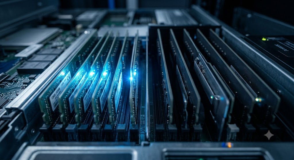
When you scale this situation to the size of a data center, the scale of waste changes. Among thousands of servers, only a fraction of nodes are under high load. Most of the memory in the remaining nodes sits idle while consuming electricity. Theoretically, there is enough total capacity, but specific nodes experience memory shortages. So, they buy more memory—while leaving the idle memory as it is.
CXL switches dismantle this structure. In a CXL-based memory pooling architecture, physical memory is bundled into a single shared resource pool via virtualization switches. If Node B needs memory, it is allocated instantly from the pool in 1GB increments, and when the task is finished, the memory returns to the pool for other nodes to use.
This has significant implications for server capacity planning. In the traditional method, memory had to be over-provisioned to handle peak loads. Since it wasn’t used simultaneously, each node had to have enough memory for the worst-case scenario, and that excess was the very definition of stranded memory.
Empirical data shows that the capital expenditure (CAPEX) for building equivalent usable memory can be reduced by up to 50 percent in a CXL pooling environment. This is because, instead of filling every individual node with ultra-high-density RDIMMs, companies can lower purchase costs by distributing relatively cheaper, general-purpose 64GB RDIMMs into CXL PCIe expansion slots.
Operating cost structures change as well. CXL physical controllers include power management circuits that detect traffic density in microseconds. When data flow subsides, it switches the link to an ultra-low-power state and recovers in nanoseconds when the next request arrives. According to mass-production data from Samsung Electronics, this mechanism reduces the idle standby power of memory modules by more than 50 percent.
Add inline hardware compression to this, and the results are even better. If DenseMem compression IP from ZeroPoint Technologies is packaged within the same die as a CXL 3.1 controller, data compression and decompression are handled automatically by the hardware accelerator. It compresses data stored in physical memory at a ratio of up to 3-to-1 without using any CPU resources.
The result is somewhat paradoxical. Even without increasing the physical number of memory chips, the logical memory capacity recognized by the operating system triples. Because the size of signal packets passing through the bus is also reduced, transmission power is lowered once more. It is a structure where CAPEX, OPEX, and power costs are reduced simultaneously. This is why CXL is more than just a performance specification.
To translate these numbers into a tangible scale: consider a hyperscaler operating 10,000 GPU servers. Cutting memory CAPEX in half means they can either expand their server count significantly with the same budget or maintain the same server scale with half the memory budget. Either way, capital that was tied up in idle memory is liberated. Until now, that capital was just sitting there, eating electricity.
The Path Samsung Walked First
Before CXL moved from academic discussion to actual product, one company made the first move.
In May 2021, Samsung Electronics developed the industry’s first CXL 1.1-based CMM-D (CXL Memory Module-DRAM). At the time, most server companies classified CXL as a technology for after 2025. Samsung had already created a physical product before then.
In May 2022, the second-generation CMM-D 2.0, which natively applied the CXL 2.0 specification, entered the mass production stage. It supported up to 256GB per single slot and provided a stable effective bandwidth of 36GB/s.
The next step, CMM-D 3.1, is based on the PCIe 6.0 interface, providing 1TB of memory space in a single module with bandwidth reaching 72GB per second. This figure is not just a spec increase. It means that a single CXL slot is beginning to exceed the total bandwidth limit of memory channels directly connected to existing CPU sockets.
SK Hynix chose a different path. At the Global Flash Summit in March 2026, they unveiled the next-generation CMM-DDR5 module and simultaneously released the HMSDK (Heterogeneous Memory Software Development Kit) as open source. It was a declaration that they would not just sell hardware. They intend to build an ecosystem where developers can directly control heterogeneous memory pools via software.
Micron is accumulating commercial reliability data by passing validation cycles in data centers with its CXL 2.0-compatible CZ120 series developed in 2023. All three companies are climbing the same mountain from different directions.
Nvidia announced that its Vera CPU, scheduled for release in late 2026, will feature CXL 3.1 as a standard. Intel’s 5th Gen Xeon and AMD’s EPYC Turin already support CXL 2.0 or higher, and Google is actively deploying CXL physical interconnects in its global data centers.
The stage where the market was waiting for standards has passed. We have entered the stage where standards are creating the market. According to industry estimates, the global CXL market is expected to grow to approximately $15.8 billion by 2028. The 2024 estimate was $1.2 billion. That is a thirteen-fold increase in four years.
Why Korea Can Compete in This Fight

New standards redraw the technology map. Previously advantageous positions become less so, and previously blocked access roads open up.
For a long time, the Korean semiconductor industry has had an unbalanced structure. While DRAM manufacturing capability is world-class, it has been difficult for domestic companies to reach the top tier in the fabless sector (creating core design IP), high-value-added packaging (OSAT), and precision inspection equipment. It was a country that made good DRAM, but not one that led the semiconductor ecosystem.
CXL shakes this structure. New interconnect standards require new chips. Switch chips, controller chips, PHY IP, inspection equipment, high-layer boards. In these areas, Korean companies are taking unexpectedly prominent positions.
Panmnesia, a startup founded primarily by KAIST researchers, developed the world’s first CXL 3.2 full-spec single switch chipset that fully executes port-based routing. This chip, named the ‘PCIe 6.4-CXL 3.2 Fusion Switch,’ connects CPUs, GPUs, accelerators, and shared memory devices within a single physical semiconductor into a composable shared system. It reduced latency overhead generated when passing through switch hops to under double-digit nanoseconds and embedded KV (key-value) cache processing—a major bottleneck in generative AI inference—as internal hardware acceleration circuitry. It won the Best of Innovation award at CES 2025 and has secured 80 billion won in Series A funding, pushing its cumulative enterprise value past 340 billion won.
MetisX, founded by veterans from Samsung and SK Hynix’s architecture design divisions, started from a different question: instead of moving data to a CPU or GPU for calculation, why not calculate directly inside the memory? They realized this concept, called ‘Computational Memory,’ on a CXL 3.0 architecture. By embedding a vector calculation engine and data compression/filtering circuitry within the CXL memory module’s controller chipset, large-scale data filtering required for AI vector similarity calculations or RAG (Retrieval-Augmented Generation) is completed within the memory device, and only the processed results are passed to the processor. Since the amount of data traveling back and forth on the bus is fundamentally reduced, processor heat decreases, and cooling costs go down as well. They raised 60 billion won in Series A and are conducting joint engineering with global cloud companies.
DeNoTesia designed a VDPU (Vector Data Processing Unit) dedicated to processing vector database tasks—converting text, images, and audio into high-dimensional numerical vectors and calculating similarity—which are essential for generative AI’s RAG and long-term memory implementation. They are commercializing their ‘Seahorse’ platform, which controls the VDPU in the cloud, and are conducting IP licensing sales to multinational SoC manufacturers and board designers by aligning their VDPU with CXL interconnect logic.
There is also a way to benefit from the ecosystem without selling chips directly: selling design assets (IP). Openedges Technology is a publicly traded IP specialist that supplies on-chip interconnect IP, memory controller IP, and PHY IP to the global market. They hold DDR5/LPDDR5X IP that any domestic or international foundry customer looking to mass-produce CXL-based controller chipsets must license. It is a structure where royalties accumulate whenever a chip is made, and 2025–2026 is analyzed as the threshold for this.
The Tester Controls Quality
As important as making chips is verifying that the chips actually work properly.
Every time a new standard emerges, a new inspection equipment market opens. Existing DDR5 inspection equipment cannot properly see CXL modules. The protocols are different, the speeds are different, and the required test conditions are different.
Neosem is the company that filled this gap first. In 2023, they commercialized the industry’s first CXL 1.1 standard inspection platform, and subsequently completed the localization of high-speed, high-temperature burn-in inspection equipment compatible with the CXL 2.0 specification, becoming the exclusive supplier of the first commercial equipment to Samsung Electronics.
Neosem’s inspection method differs because of the extremity of its operating conditions. While the memory is actually running, they apply thermal stress by raising and lowering the chamber temperature to the extreme, tracking defects in real-time. There are chips that operate normally at room temperature but reveal errors only during temperature changes; their work is to catch those errors before shipment.
For a long time, the global semiconductor inspection market has been dominated by Teradyne of the US and Advantest of Japan. These two companies have effectively defined inspection standards first for every DDR generation. Neosem succeeded in delivering mass-production inspection equipment before these two giants in the new CXL standard. In the short gap where standards change, the order has been reversed.
Exicon is focusing on developing CXL 3.0-specialized memory modules and protocol analysis equipment applying Samsung Electronics Foundry’s 4nm process, and is promoting customer diversification by establishing a Silicon Valley branch based on its PCIe interface analysis patents. Fadu is conducting field tests of controller chipsets compatible with CXL physical protocols and FPGA-based proof-of-concept cards. Qualitas Semiconductor has secured PHY design assets compatible with PCIe 6.0/CXL 3.1 that deliver speeds of over 64GT/s without physical noise, and is conducting early validation with global system semiconductor firms.
Without a Substrate, a Chip is Adrift
A semiconductor chip is not a finished product by itself. It only works when mounted on a foundation called a substrate. CXL high-speed signals require special conditions for the substrate. For signals of 64GT/s or higher to pass without distortion, the substrate material and lamination design must be different from standard server substrates.
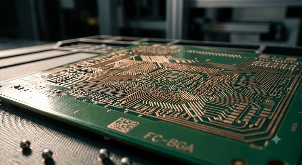
TLB is a company that first secured high-frequency, lossless signal transmission layer design for CXL modules and next-generation low-power LPCAMM-specific module substrate process technology. To respond to surging global demand, they started operations at their second plant in Vietnam early and achieved single-digit ppm yields using AI-controlled automation robots. They are also a key partner to both Samsung Electronics and SK Hynix.
Daeduck Electronics is a packaging board manufacturer that has finished expansion investments for FC-BGA (Flip-Chip Ball Grid Array) large-scale packaging substrates. Because product unit prices jump as bump bonding density becomes finer and multi-layering progresses, they are in a position where the higher the technical barrier, the greater the benefit.
When listed this way, it looks like a complete value chain. There are switches, controllers, inspection equipment, and substrates. But for these pieces to actually interlock and function, one more step remains.
The Real Fight Starts Here
Technology seems already in place. There are chips, switches, inspection equipment, and substrates. Standards are set.
Then why is CXL not yet the mainstream of the server market? There are many reasons, but one unexpected point stands out: the cost of software design tools.
EDA (Electronic Design Automation) software, monopolized by multinational firms like Synopsys or Cadence, is an essential tool for semiconductor design. License costs range from hundreds of millions to billions of won annually. Even if startups like Panmnesia, MetisX, and DeNoTesia have created world-first technologies, they must continue to use this software to design the next generation of chips. For a startup before significant mass-production revenue, this cost is a financial chokehold.
The team that developed the world’s first technology stops because they can’t afford to rent the tools to draw the next chip.
This is not a technical problem. It is a structural one.
What the Ministry of Science and ICT and the Ministry of SMEs and Startups must do right now is not to split up and distribute government subsidies. They must drastically increase the tax deduction limit for EDA software procurement costs and operate a long-term lease support guarantee fund on a regular basis. Institutional mechanisms are also needed to prioritize the allocation of MPW (Multi-Project Wafer) slots from Samsung Electronics and SK Hynix foundries to domestic small-to-medium fabless firms.
Without that, the teams that develop world-first technologies will repeatedly be sold to foreign capital or absorbed by foreign fabless firms at the mass-production stage. We will see cases where the country that first created the switch chip is missing from the mass-production stage.
New rules are being written right now regarding how humanity will design AI infrastructure. Korean companies are sitting at the table where those rules are being written for the first time.
If you look at this fight only at the company level, you only see half the picture. The power consumption of a single data center has now grown to the scale of a small city, and there are increasing cases where the possibility of grid connection in new data center construction permits is a condition that precedes site selection. Utility companies and local governments have effectively ended up in a position where they coordinate the speed of AI infrastructure expansion.
In this picture, the position of CXL is subtle. Technology that reduces memory bottlenecks to process the same computation with less power is one of the few solutions that can be implemented faster than building new power plants. This is where the problem of semiconductor design connects to national power planning. When Microsoft first mentioned electricity shortages, that statement was already spreading into a problem for power grid operators, not just GPU companies.
Beyond the Memory Wall
Thirty years ago, there was a problem given a name: the Memory Wall. There have been constant attempts to cross that wall. We made faster DRAM, connected more channels, and stacked chips with higher density. The wall did not disappear.
Because the architecture itself was creating that wall.
CXL is an attempt to change the architecture. It breaks down the boundary between memory and processor, creates physical lines where reads and writes flow simultaneously, and turns memory that was trapped in fixed nodes into shared resources.
What comes when this change is complete is not faster AI. It is a world where we can use more AI with less electricity.
If the real barrier to AI infrastructure expansion right now is not land but the power grid, and if a significant portion of that power waste comes from the time data spends waiting, then the problem CXL solves is not a technical problem, but an energy problem.
If we can move data more efficiently, we can provide AI to more people at a lower cost. Part of the response speed and subscription fees of the AI service you use right now is leaking from this memory bus turnaround penalty.

For thirty years, the industry has been running toward stronger processors. The wall appeared in a different place every time.
Where will the next wall be? And how long will it take us to notice that wall?
References
- CXL Consortium Technical Working Group. CXL 2.0 and 3.0 Specification Standard White Paper. Compute Express Link Official Technical Document Repository. 2022–2024.
- KAIST Next-Generation Memory System Joint Research Center. Performance Analysis of Memory Hierarchy and CXL Interconnect for Next-Generation High-Bandwidth Computing. Journal of the Korean Institute of Electrical Engineers. 2023.
- Samsung Electronics Memory Business Unit New Business Strategy Team. CMM-D Product Line Technical Roadmap and Value Assessment for Overcoming Data Center Memory Bottlenecks. Samsung Semiconductor Technical White Paper Series. 2022–2024.
- ZeroPoint Technologies; Rambus Joint Research Team. Analysis of Total Cost of Ownership (TCO) and Power Efficiency Models in CXL Memory Pooling Environments. IEEE Computer Architecture Letters. 2024.
- Noh Geun-chang et al. Analysis Report on Korean System Semiconductor Companies' Preemption of Heterogeneous Computing Paradigms. Hyundai Motor Securities Industry Analysis Report. 2024–2025.
- SK Hynix Solution Development Center Software Lab. Technology Trends in HMSDK and Open Source Control Stacks for Heterogeneous Architectures. SK Hynix Technical Seminar Presentation. 2026.
- Wulf, Wm. A.; McKee, Sally A. Hitting the Memory Wall: Implications of the Obvious. ACM SIGARCH Computer Architecture News. 1995.
- NVIDIA Corporation. Vera CPU Architecture Overview and CXL Integration Roadmap. NVIDIA GTC Technical Proceedings. 2025.
- Intel Corporation. 5th Gen Intel Xeon Processor Platform: CXL 2.0 Implementation Guide. Intel Developer Zone Technical Documentation. 2024.
- AMD Corporation. EPYC Turin Architecture: Memory Subsystem and CXL Controller Design. AMD Developer Resources. 2024.
- Google Infrastructure. Hyperscale Memory Disaggregation with CXL: Early Deployment Data from Production Workloads. Google Research Technical Report. 2025.
- Rambus Inc. PCIe 6.0 Physical Layer Controller for CXL 3.1: Performance and Power Characterization. Rambus Product Technical Documentation. 2024.
- Panmnesia. PCIe 6.4-CXL 3.2 Fusion Switch: Low-Latency Composable Memory Architecture. CES 2025 Innovation Award Technical Submission. 2025.
- MetisX. Computational Memory Architecture on CXL 3.0: Near-Memory Processing for AI Vector Workloads. Hot Chips Symposium Proceedings. 2025.
- Neosem. CXL 2.0 Module Burn-in Test Solution: Field Validation Report for Next-Generation Memory Qualification. Semiconductor Equipment Technology Council Presentation. 2024.