
The Wires Are Clogged
Throughout 2025, the world’s largest cloud companies poured hundreds of trillions of won into capital expenditures for data centers.
A single NVIDIA H100 chip costs over 40 million KRW. When you bundle thousands of these into a cluster, the costs balloon into the hundreds of billions of won almost instantly. People assume most of this money goes into the compute chips.
They are wrong. The most expensive part isn’t the chip; it’s the time the chips spend waiting for each other.
When thousands of GPUs train a single neural network, they must exchange intermediate calculations at every step. If one device finishes its task but doesn’t receive a synchronization signal from another, it cannot move to the next stage. The industry calls this waiting state a ‘Stall.’ And these stalls aren’t caused by the chips—they are caused by the wires.
Specifically, it happens at moments like this:
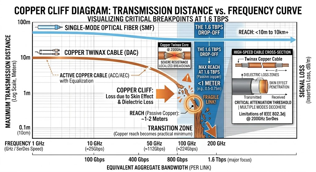
At the next-generation 1.6 Tbps transmission standard, the effective transmission distance of copper cabling collapses to under 1 meter due to the laws of physics. However, the average height of a server rack is over 2.5 meters. We have reached a point where it is physically impossible to even run a cable from the GPU at the bottom to the network switch at the top of the same rack. The industry calls this phenomenon the ‘Copper Cliff.’
Optical cables, suggested as an alternative in the face of this cliff, solve the distance issue but require 15–20W of power per port. In hyperscale data centers running tens of thousands of ports, this translates directly into massive electricity bills and carbon emissions.
Copper is too short, and light is too expensive. In the gap between this binary choice, plastic has emerged.
The First Wall: Copper Swallows High Frequencies
The Physics of the Skin Effect
Why does copper cabling suddenly become useless? The answer lies not in materials science, but in electromagnetics.
When alternating current flows through a conductor, as the frequency increases, the charge is pushed away from the center of the conductor toward the surface. This ‘Skin Depth (δ)’ phenomenon is inversely proportional to the square root of the frequency f.
δ = √(ρ / πfμ₀μᵣ)
In plain terms, when the frequency quadruples, the effective cross-sectional area through which current can flow is halved. As the area decreases, resistance increases, and as resistance increases, the signal is lost as heat. In the ultra-high frequency band of 100 GHz and above, a copper conductor functions less like a signal transmission medium and more like a heater that incinerates the signal. This is why the effective distance of passive copper cables cannot exceed 1 meter in a 1.6 Tbps transmission environment, and this distance shrinks even further in the 3.2 Tbps generation.
A World After the ‘Copper Cliff’
Field engineers have been managing this limit by using thicker cables. While thicker wires reduce resistance, the cables become heavy and rigid, clogging the rear of server racks. If the exhaust vents are blocked, cooling efficiency drops and internal temperatures exceed critical thresholds. The weight and stiffness of the cables can even physically damage port connectors.
An emergency fix for this problem is the Active Electrical Cable (AEC). By attaching a signal regeneration chip (retimer) to the end of the cable, the reach is extended to 2–2.5 meters. But that is the limit. It is still insufficient to meet the wiring requirements of 1.6 Tbps generation data centers.
The evolution of copper cabling has already hit the ceiling of physical laws. There can be no faster or thinner copper cables. All that remains is higher frequencies and the resulting ever-narrowing effective cross-sectional area of the conductor.
The Second Wall: Light Is Expensive
The Costs of Optical Fiber
Because optical fibers transmit signals through light refraction rather than electromagnetic loss, they are completely free from the skin effect that plagues copper. They can easily cover distances in the kilometer range. So, why don’t hyperscale data centers switch entirely to optical cables?
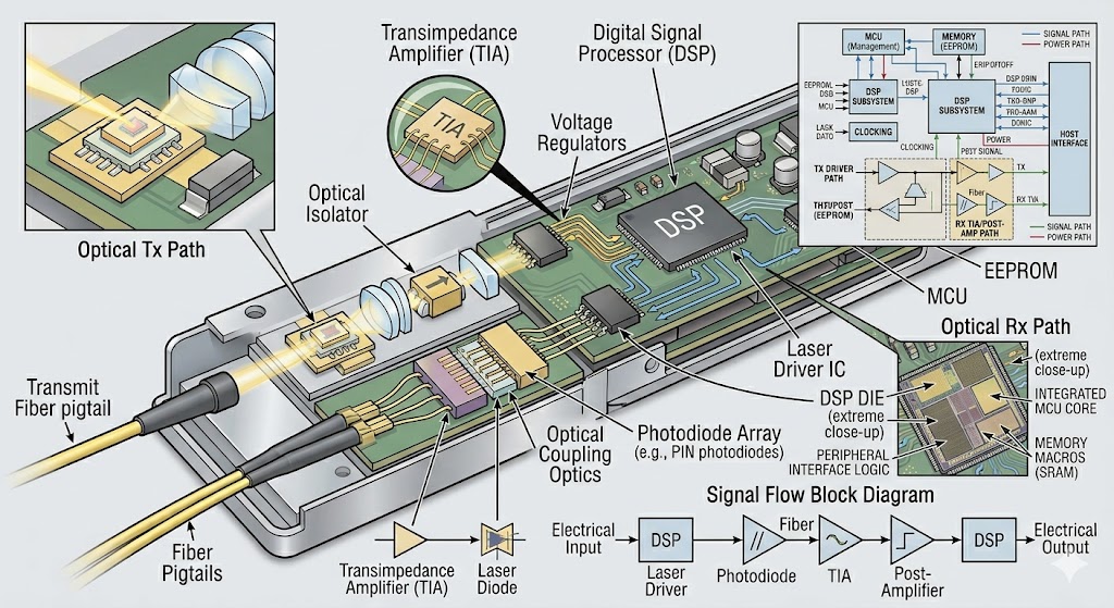
To convert electrical signals into light, you need hardware. A laser diode fires light, a driver modulates it, an optical DSP restores the signal, and a transimpedance amplifier (TIA) at the receiving end converts it back into voltage. This combination of components is the optical transceiver module.
An 800 Gbps optical transceiver consumes an average of 15–20W. In a massive data center with tens of thousands of ports running simultaneously, the power consumed by just one interconnect layer is equivalent to that of a giant power plant.
Cost is also an issue. Optical transceivers require indium phosphide (InP) or gallium arsenide (GaAs) compound semiconductors and silicon photonics packaging, making them 4–10 times more expensive than equivalent passive copper cables.
Reliability is another weakness. Laser diodes age quickly in high-temperature, high-humidity environments, and the thermal shock near server rack exhaust vents further shortens their lifespan. In distributed parallel computing, a single connection failure can stop an entire training session, forcing a restart from the previous checkpoint. It actually happens that training sessions running for days on thousands of GPUs are wiped out by the failure of a single laser in an optical transceiver.
The Limits of Co-Packaging
Co-Packaged Optics (CPO) is an attempt to solve this by placing the chip and optical components in the same package. It minimizes the distance electrical signals travel on the substrate, thereby increasing power efficiency. However, CPO dramatically increases the complexity and cost of the manufacturing process. Integrating silicon logic and optical components into a single package is a challenge in semiconductor manufacturing, and above all, it does not eliminate the fundamental energy inefficiency of electro-optical conversion.
The Third Material: Plastic Swallows Millimeter Waves
In 2014, an idea from a KAIST research lab attacked this binary dilemma head-on. It uses no copper and no lasers. The concept was to fire electromagnetic waves into a plastic tube.
Developed by Point2 Technology, ’e-Tube’ is a system that confines and transmits RF signals in the millimeter-wave (100–260 GHz) band inside a specially molded, low-loss polymer resin dielectric waveguide.
Since there is no conductor, the skin effect does not occur at the source. Since there is no laser, there is no electro-optical conversion loss or risk of laser degradation.
What Happens Inside the Waveguide
While the physics of a dielectric waveguide is similar to that of optical fiber, the signal being confined is different. While optical fiber confines light at visible light frequencies (hundreds of THz), e-Tube confines electromagnetic waves at millimeter-wave frequencies (hundreds of GHz).
The principle is Total Internal Reflection. A plastic core with a high refractive index is surrounded by cladding with a low refractive index. The injected electromagnetic waves cannot cross the boundary and propagate along the core. In this structure, signal attenuation is determined solely by the dielectric loss tangent (tan δ) and the dielectric constant (ε) of the plastic material, not by high-frequency metal resistance.
α_dielectric ∝ f · √ε · tan δ
Crucially, unlike copper, the rate at which attenuation increases as frequency rises is much slower than in metal. This is the physical basis for signals being able to travel stably for 10–20 meters even in the ultra-high frequency bands required by the 1.6 Tbps and 3.2 Tbps generations.
From TX Chip to Waveguide: The Role of the MWT Antenna
Computer systems operate on baseband digital signals. If these signals are fed directly into a dielectric waveguide, the low-frequency components leak through the boundaries and fail to propagate.
Therefore, Point2 Technology placed a proprietary RFIC chipset inside the plug at the end of the cable.
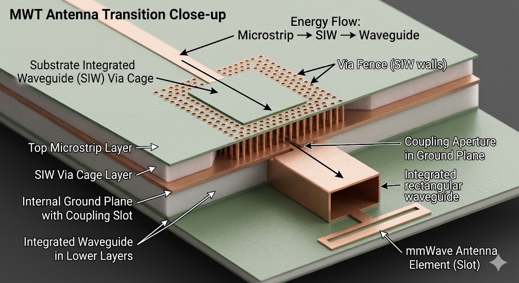
When the transmission chip (TX SoC) receives a baseband digital signal and upconverts it into a 100–260 GHz millimeter-wave analog RF signal, a ‘Microstrip-to-Waveguide Transition (MWT) antenna’ etched onto the chip surface fires the signal into the e-Tube.
The MWT matches the planar electrical impedance of the silicon substrate to the three-dimensional electromagnetic impedance inside the dielectric, ensuring the electromagnetic wave is injected into the center of the waveguide core without energy reflection or external leakage.
On the other side, the receiving chip’s (RX SoC) on-chip antenna captures the arriving electromagnetic wave and uses a downconversion mixer to restore it to the original digital bus signal. The host ASIC—such as a GPU or switch—doesn’t even need to be aware that an e-Tube is in the middle.
The Number 80 Picoseconds
The result of this analog conversion path is a latency of 80 picoseconds (ps). Optical cable systems using optical transceivers experience latency in the microsecond (μs) range due to electrical-to-optical conversion, digital signal processing, and optical-to-electrical conversion. e-Tube’s latency is 1,000 times lower.
In distributed parallel computing, latency is not just a speed metric. When thousands of GPUs perform synchronized calculations, the slowest link determines the processing speed of the entire cluster. This is why 80ps of latency has 1,000 times the significance.
Comparison Table by Numbers
Looking at five different interconnect technologies side-by-side makes the picture clear.
e-Tube fills the void between the distance copper has given up on and the cost optics cannot handle. Designing for rack-level server wiring in the 10–20 meter range is the goal of this technology.
The Company’s Roots and Two Cash Cows
Point2 Technology was founded in March 2014. It was co-founded by CEO Sean Park, who led high-speed communication system chip design at Marvell and TeraSquare for over 13 years, and Professor Hyun-Min Bae of KAIST’s School of Electrical Engineering (current President of KAIST Startup Institute) along with his master’s and doctoral research team. The company has a dual structure, with its headquarters in San Jose, California, and core R&D handled by a Korean subsidiary.
It took time for e-Tube to establish itself in the market. Two business lines fill the gap in the meantime.
25G Range Extender: The Hidden Bottleneck of 5G Base Station Networks
In 5G communication networks, the fronthaul optical links connecting base stations to core networks are being upgraded from 10 Gbps to 25 Gbps. This creates an unexpected problem.
‘Chromatic Dispersion,’ a phenomenon where the refractive index within an optical fiber varies by wavelength, distorts signals in proportion to the square of the frequency ratio. An optical line that comfortably covered 70–80km at 10 Gbps sees its effective distance collapse to 15km at 25 Gbps. It is a paradox where faster transmission results in shorter reach.
The traditional solution was to install massive, expensive external dispersion compensation filter devices at every relay point, with technicians manually adjusting them according to line length. Point2 Technology’s range extender solves this with a semiconductor chip the size of a fingernail inside the optical transceiver module. An Electronic Dispersion Compensation (EDC) engine restores the completely collapsed eye pattern in real-time, returning the effective transmission distance to 60–70km. No external devices or field adjustments are needed. You simply replace the optical transceiver.
Based on this technology, Point2 Technology signed a long-term development partnership with Japan’s Sumitomo Electric Industries and secured a contract for the mass production of 25G optical transceiver core ICs. This is the company’s first cash flow.
Smart Retimer P1B121: Half the Power, 1/20th the Latency
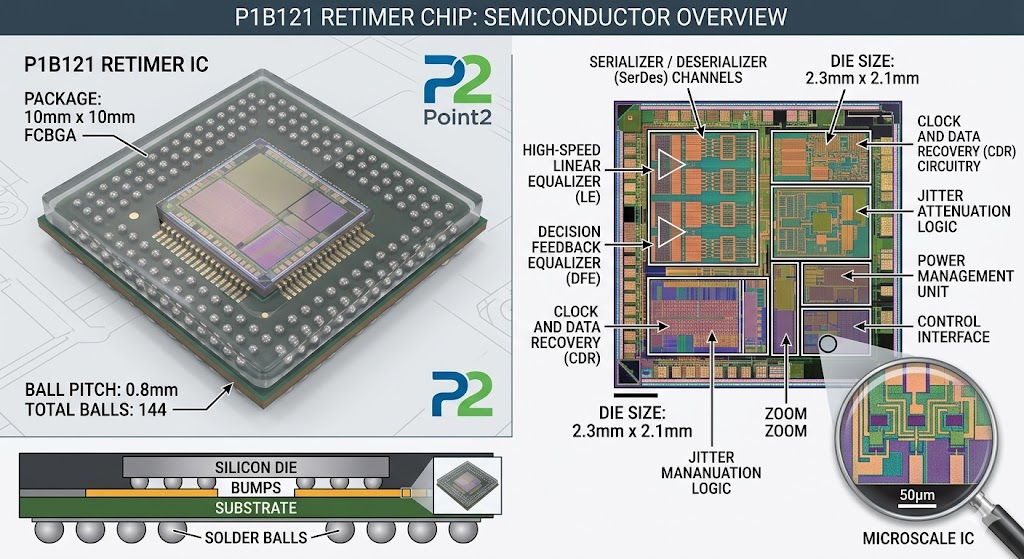
The second cash cow is the 112G PAM4 smart retimer chipset ‘P1B121’ for data centers. A retimer is a chip that cleans and regenerates distorted signals at the ends of high-speed electrical cables; it is essential for next-generation 800 Gbps and 1.6 Tbps Active Electrical Cables (AEC). The problem is that competitors’ products consume too much power.
The P1B121 achieves 3.0W driving power, about 50% lower than comparable competitors. The latency is also less than 3 nanoseconds (ns), which is 1/20th of the industry average. This is the result of mixed-signal optimization design that maximizes analog signal path processing. 3W and 3ns—these two numbers mean more than just digits. They prevent the retimer’s latency from becoming a bottleneck in large-scale accelerator clusters that require ultra-low latency synchronization, while simultaneously providing headroom in the power budget.
Why NVIDIA Invested Directly in Korea
In 2024, an unusual event occurred in the global semiconductor market. NVIDIA’s strategic venture capital arm, NVentures, made its first-ever direct equity investment in a Korea-based semiconductor startup. The target was Point2 Technology.
NVentures is an organization that executes strategic investments not for financial gain, but to strengthen NVIDIA’s future platforms and technology ecosystem. It can be read as a move to incorporate the e-Tube transmission layout as a core backbone for the scale-up fabric of next-generation accelerator architectures following Blackwell.
Including this investment, Point2 Technology has completed a cumulative $76 million (approximately 112.1 billion KRW) Series B funding round. Maverick Silicon led the round, with participation from UMC Capital, Bosch Ventures, and Molex. The list of investors suggests a strategic ecosystem building rather than simple financial support.
The participation of global automotive parts giant Bosch hints at the possibility of e-Tube entering the automotive market. The investment from cable manufacturer Molex is an example of a production partnership turning into a capital relationship. The 2026 BloombergNEF Pioneers award is external validation of this technology.
The Fabless Paradox: How to Dominate the Global Supply Chain Without Factories
Point2 Technology does not own manufacturing plants. That is the strategy.
They do not make finished e-Tube cables themselves. Instead, they design the RFIC chipsets that control electromagnetic modulation and provide the geometry and bonding design technology for e-Tube waveguides under license. Actual production is handled by the world’s largest connector manufacturers.
Molex, Foxconn Interconnect Technology (FIT), and Amphenol. These three companies are proven vendors that have already supplied trillions of won in volume to the data center supply chains of Amazon AWS, Google Cloud, Microsoft Azure, and Meta.
For Point2 Technology to enter the hyperscaler supply chain directly, it would have to pass years of rigorous supplier audits. However, by shipping finished Active RF Cable (ARC) products—which embed the e-Tube chipset—via the brands and logistics networks of already-listed partners, they can shorten this process.
They only do chip design. Manufacturing is done by partners who have already built trust. Channels are also those of the partners. This is the secret to why the fabless model generates high operating profit margins.
Changes in Revenue Mix Toward 2030
Currently, Point2 Technology’s cash comes from the 25G range extender and smart retimers. This is the fuel keeping the company running today. However, the direction the company has mapped out points elsewhere. The core of their internal roadmap is to shift 90% of total revenue to e-Tube-based product lines by 2030.
There is a market structure supporting this transition. Between 2026 and 2028, global data centers will transition in earnest to 1.6 Tbps and 3.2 Tbps generations. At this point, copper cables will inevitably be completely replaced by ARC (Active RF Cable) or optical cables due to physical limitations. This is the size of the replacement market e-Tube is targeting.
Beyond the external cable stage, deeper integration awaits. Near Package e-Tube (NPE) brings ultra-thin e-Tube waveguides into close proximity with the silicon interface inside the accelerator board. Co-Packaged e-Tube (CPE) is a structure that integrates RFIC components inside the GPU packaging substrate itself. At this stage, noise from copper wiring on the board disappears, and electromagnetic waves are launched directly from the accelerator chip into the dielectric tube.
Information that they have signed non-disclosure MOUs with at least one top-tier global GPU manufacturer and are preparing for a prototype demo in the second half of 2026 suggests that this roadmap is not just a declaration but is in the execution phase.
e-Tube’s infiltration path does not stop at data centers. Whether it’s terabit-grade signal wiring inside ultra-thin premium display panels or noise-shielding wiring between autonomous driving ECUs and multi-channel sensors, the physical principles of e-Tube apply wherever electromagnetic interference is a problem and space is limited.
KOSDAQ IPO: Where Does It Actually Stand?
When I first wrote this, Point2 Technology’s goal was to apply for a preliminary KOSDAQ technology special listing review in the second half of 2026. However, checking again a few months later, that schedule has not been maintained.
According to the most recent reports, the company’s target time for listing has been pushed back to “as early as next year, or as late as the year after.” That means between 2027 and 2028. Because the headquarters is a US corporation, there is even talk of shifting the direction toward global capital markets like NASDAQ instead of KOSDAQ. The underwriters are still a joint system of Samsung Securities and Korea Investment & Securities, and the figure for the target corporate value at listing of over 1 trillion KRW remains the same.
The background for the delayed schedule is not significantly different from what was initially known. The cross-border governance structure between the US San Jose headquarters and the Korean subsidiary became a hurdle. Aligning the profit-oriented corporate governance requirements of US federal law with the technology special listing lock-up requirements and cross-border equity settlement structures of the Korea Securities Depository and Korea Exchange required a longer adjustment period than expected.
Funds raised through a pre-IPO round just before listing are planned to be prioritized for foundry initial mass wafer production deposits and expanding local US engineering support infrastructure. The fact that the company’s IPO schedule itself is being delayed shows that just because a technology is verified doesn’t mean the IPO clock speeds up on its own.
Wires Make Technology Invisible
Let’s stop here and think.
The problem e-Tube solves is interesting in that technology works properly only when it doesn’t reveal itself. The best interconnect solution has no presence. A GPU doesn’t care what the cable is made of. The host system doesn’t even realize that electromagnetic waves passed through plastic in the middle.
This is the essence of infrastructure. Infrastructure works best when it is invisible.
However, there are moments when infrastructure suddenly becomes visible. It happens when wires are clogged, power budgets are exceeded, or latency drags down the entire cluster. The data center industry is standing exactly at that point right now. Copper is blocked, optics are too expensive, and AI keeps demanding faster things.
The moment infrastructure is revealed by crisis is the condition that allows a new material to step in. The fact that plastic dielectrics have created a third space between copper and optical fiber is not just a story about a better cable being invented. It is about redesigning the physical constraints of AI infrastructure.
It is common to hear that AI will change the world. Stories about what material the wires running that AI are made of are rare. But if a single wire determines the actual performance of a multi-trillion won cluster, the question about the company making that wire is no different from a question about the future of AI infrastructure.
References
- Point2 Technology Inc. — e-Tube RF Dielectric Waveguide Architecture White Paper (2024)
- Why E-Tube Cables Offer a Promising Alternative to Copper and Optical Interconnects
- waveguide
- Point2 Technology Inc. — 25G Range Extender and Sumitomo Electric Partnership Technical Report (2023)
- Bloomberg NEF Pioneers — 2026 Point2 Technology Technology Assessment (2026)
- NVIDIA NVentures — Series B Investment Announcement (2024)
- IEEE Transactions on Microwave Theory and Techniques — "Dielectric Waveguide for On-Board and Short-Reach Interconnects" (2022)
- AI, data centers, and the energy equation: What business leaders should know
- IEEE 802.3 Task Force — "200G/lane Electrical Signaling and Copper Cliff Analysis" (2023)
- Home » Signal Integrity » Futuring Interconnect Infrastructure for AI: RF Transmission over Plastic Cable Surpasses Copper and Optics at Terabit Scale Signal Integrity Futuring Interconnect Infrastructure for AI: RF Transmission over Plastic Cable Surpasses Copper and Optics at Terabit Scale
- Hyperscale Data Center Market Size & Share 2026-2035
- IEC 62149 Series — Fibre Optic Active Components and Devices: Reliability Standards for Laser Diodes in Data Center Environments
- Semiconductor Business Models: Fabless and Fearless
- Point2 and FIT partner on terabit-speed interconnects