
1,300 soccer fields. 50 times the size of the Pentagon.
In Grimes County, Texas, next to the Gibbons Creek Reservoir, a structure of that magnitude is rising from the farmland. Once completed, it is slated to be the largest and most expensive structure on Earth.
Yet, there is something strange about it. The factor identified as the key to this project’s success is not concrete. It’s not the steel, nor the initial $16.8 billion investment. It’s something that cannot be captured in a photograph or drawn on a blueprint. People in the semiconductor industry simply call it “culture.”
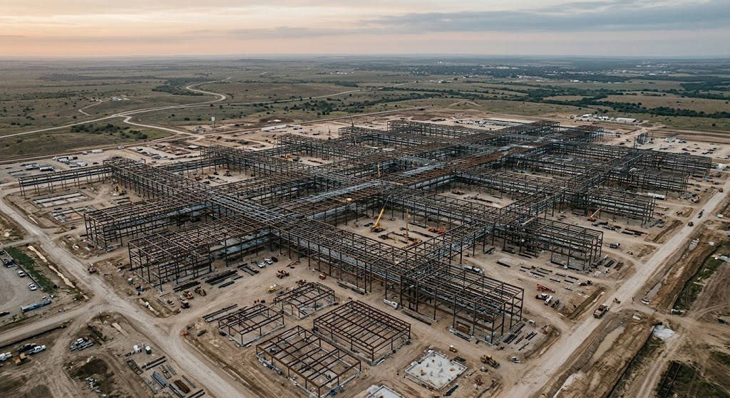
This building is named Terafab. It is a joint project involving Tesla, SpaceX, and xAI. The goal is to churn out 1 terawatt—or 1,000 gigawatts—of AI computing hardware annually. Even if you combine the current cutting-edge semiconductor production capacity of the entire world, it falls short of this number. Wall Street estimates suggest that the combined output of all AI-dedicated fabs currently operating globally is around 20 gigawatts. Terafab aims to handle 50 times that output on its own.
You might ask why this matters to you. The answer is simple: much of the reason your AI services are slow, laggy, or seeing new model releases delayed is ultimately due to a chip shortage. The high cost of cloud GPU rentals and the difficulty of lowering prices for new smartphones and laptops are for the same reason. Robots, autonomous vehicles, and satellite internet are all stuck behind this bottleneck.
The fact that you have to wait weeks to rent a single GPU and that new AI services are launched sequentially by region are consequences of this same bottleneck. As computing power becomes a scarce resource, a dynamic is hardening where only the services of companies that secure that resource first function smoothly. Terafab’s vision is to flip this dynamic. It implies that the gap between companies that make their own chips and those that cannot could widen significantly.
Terafab is a declaration to resolve that bottleneck entirely. If successful, the price and speed of AI hardware will change. If it fails, the scale of that failure will also be the largest on the planet.
For Musk, this project means more than just securing a supply chain. At a public event last March, he described Terafab as “the next step toward becoming a galactic civilization.” Even his vision of building a base on the moon and running petawatt-scale computing there with solar power is an extension of this project. The 1-terawatt goal itself exceeds South Korea’s total power generation capacity by several to ten times. It is a target set not by a country, but by a single company—one that has never mass-produced semiconductors before.
Why Money Can’t Solve It
In biology, there is a long-standing distinction regarding reproductive strategies. One is the r-selection strategy: producing as many offspring as possible quickly with minimal investment. Insects and fish do this. It is an advantageous strategy when the environment is harsh and unpredictable.
The other is the K-selection strategy: pouring long-term time and resources into a small number of offspring. Elephants do this. Their gestation period alone is 22 months, and calves stay with their mothers for over a decade until they are fully independent. It takes time to reach adulthood, but survival rates are correspondingly higher.
Advanced semiconductor manufacturing is closer to the latter. A single wafer goes through hundreds of process steps. Photolithography, etching, deposition, cleaning, ion implantation, chemical mechanical polishing—each step involves dozens of intertwined variables. Increasing yield by 1 percent takes months, and those months are filled not by new equipment, but by the accumulated judgment of people. When a wafer comes out defective, the intuition to distinguish whether it’s due to equipment error, chemical purity, or temperature deviation cannot be conveyed in a single manual.
TSMC is where it is today not because they bought EUV equipment earlier than others. It is because the organizational habit of working through the night to find the root cause when problems erupt has been built up over 40 years. That habit is passed to the next generation only by having junior engineers watch and absorb it from their seniors over several years. Within the industry, the diagnosis for why Intel fell behind in micro-processing is not a lack of equipment, but rather that their decision-making slowed down and their “on-the-ground” habits loosened.
Terafab is an attempt to produce the results of an elephant at the speed of an insect. Musk demanded that this project be pushed “at the speed of light.” Suppliers are asked to provide quotes on Friday and expected to reply by Monday.
The same pattern is visible in their hiring. Tesla has preferred a “speed-hiring” approach, making decisions within weeks of posting a job. In contrast, companies like TSMC or Samsung train people over several years by rotating them through various processes after hiring them as entry-level staff. If the former is an r-strategy of producing many and growing fast, the latter is a K-strategy of hiring fewer and nurturing them for a long time. The problem is that semiconductor yield itself only emerges reliably through the latter method. No matter how much you increase the speed of hiring, the time it takes for those new hires to actually develop the necessary judgment does not decrease.
The problem is that no matter how many fast-reproducing species you release, they struggle to survive in an ecosystem that requires slow maturation.
If you push this distinction further, you see an interesting point. With r-strategists, the loss of an individual doesn’t significantly harm the ecosystem because they reproduce so abundantly. Conversely, with K-strategists, the loss of a single individual is a loss to the entire lineage. If an elderly female dies in an elephant herd, the knowledge of water hole locations and how to survive droughts dies with her.
Here is an example of how this judgment actually works. In the photoresist process, where photoresist is thinly applied to a wafer, if the thickness is off by even a nanometer, the entire circuit pattern becomes skewed. A veteran engineer can pinpoint the cause of this error just by looking at a few lines of data. They use intuition to distinguish whether it is due to nozzle wear, humidity changes, or the viscosity of the raw material lot. This intuition is not summarized in papers or manuals. It only remains in the bodies of those who have experienced the same failure multiple times.
Veteran engineers at semiconductor fabs are similar. After founding the company in 1987, TSMC founder Morris Chang built an organizational culture over decades where problems were investigated until solved, even if it meant working through the night. That culture was stored in people’s bodies, not in manuals. Knowledge that is passed down only by junior engineers watching and absorbing from seniors for years is called ’tacit knowledge’ in the industry. Like the elderly female in an elephant herd, when one person with this tacit knowledge leaves the organization, that knowledge leaves with them. Even if you hire replacements, it takes years for them to acquire the same intuition.
Numbers You Can Feel
The site area for Terafab is approximately 9 million square meters. In terms of soccer fields, that’s just over 1,300. It is more than three times the size of Yeouido in Seoul. Musk stated that upon completion, the building will be 50 times larger than the Pentagon.
The investment scale has shifted every time it was announced. At the public event in March, it was introduced as a $25 billion project. By July, it had grown to $55 billion. On August 6, Reuters confirmed the first phase of investment at $16.8 billion. The company stated that once full expansion is complete, it could reach up to $119 billion. That’s nearly 170 trillion KRW buried in the land next to a Texas reservoir.
The fact that the number itself has changed three times in five months shows just how fluid this plan still is.
The compression they aim for is even clearer in other numbers. In the current semiconductor industry, it usually takes 6–9 months from designing a chip to actually printing it. Terafab claims it will reduce this cycle to a matter of weeks. The calculation is to eliminate logistics and waiting times scattered across processes by packing everything from mask production to lithography, advanced packaging, and testing under one roof.
Production capacity targets are also ambitious. The plan is to start at 100,000 wafers per month for 2nm and eventually increase to 1 million wafers per month. Wall Street analysts estimate this is close to 70 percent of TSMC’s total production capacity. A significant portion of this output is expected to be allocated to SpaceX satellites and space data centers, with the remainder going to Tesla’s self-driving and humanoid robot, Optimus. A plan to hire at least 3,000 new employees was also announced.
If you look at the numbers differently, the burden becomes clearer. Hiring 3,000 people for a single fab means you have to pull that many skilled workers from somewhere. Semiconductor process personnel cannot be deployed to the field after just a few semesters at a university. You must either poach people who have already gained experience at existing fabs or hire new people and train them from scratch. Both methods take time.
Power and water consumption are also overwhelmingly high. The 1-terawatt goal is an output that would require hundreds of nuclear power plants to run simultaneously. A single advanced fab consumes as much electricity as a small city. The impact this facility will have on the Texas power grid once completed is another variable that remains unanswered. This is why power grid and water resource security were discussed from the site selection stage.
People Moved in the Opposite Direction
Yet, the people actually moved in the opposite direction.
Jim Keller and Peter Bannon, who led Tesla’s own chip design, left the company. Milan Kovac, who led Optimus engineering, and David Lau, VP of Software Engineering, also left in 2025.
Ganesh Venkataramanan, who led the Dojo supercomputer for AI training, was no exception. In August 2025, the Dojo project itself was suspended. Musk declared at the time that the second generation of Dojo had reached an “evolutionary dead end.” The reason was that it was irrational to split resources between two different chip designs. About 20 engineers from the team left together to start a startup called ‘DensityAI’. They are now making AI chips for robots and autonomous driving, using the know-how they accumulated within Tesla in the competitive market.
While declaring they would build the fastest factory in the world, the experienced brains needed by that factory quietly stepped away. Wall Street analysts suggested that intensified competition, declining sales, and backlash against Musk’s political moves were the backdrop for this talent drain.
Of course, Dojo was revived in January 2026 under the name ‘Dojo 3’. The reason was that the new AI5 chip design had reached a stable trajectory. Musk posted a new job opening, saying he was looking for people to make the chips with the highest production volume in the world.
But a team that has been scattered and the judgment that team has built cannot simply be restored by rearranging a budget. The people who left Dojo are now under different roofs, making chips for other companies with the intuition they built at Tesla.
An Attempt to Transfer Culture Along with People
Musk’s chosen solution, in the end, was people. In July, Tesla recruited Gary Jiang, who had worked at Intel for nearly 18 years, as the Director of Terafab.
Gary Jiang majored in materials science at Tsinghua University and began his career at Rudolph Technologies, a semiconductor metrology equipment company. At Intel, he oversaw the work of transferring technology from the development fab in Oregon to the mass-production fab in Arizona. He is a key figure who led the fab transfer of the so-called 18A process. He is considered one of the few people with the know-how of ‘fab replication’—quickly stabilizing a new fab to the same yield as existing lines.
There is a reason why one person’s job change is exceptional. It is extremely rare for key talent in advanced processes to move to a competitor, especially without major industry backlash. What he moved wasn’t just a resume. It was the judgment itself, accumulated over 18 years in Intel’s cleanrooms while tracking the causes of failed lots. It is an attempt to transfer organizational culture by loading it onto a single person.
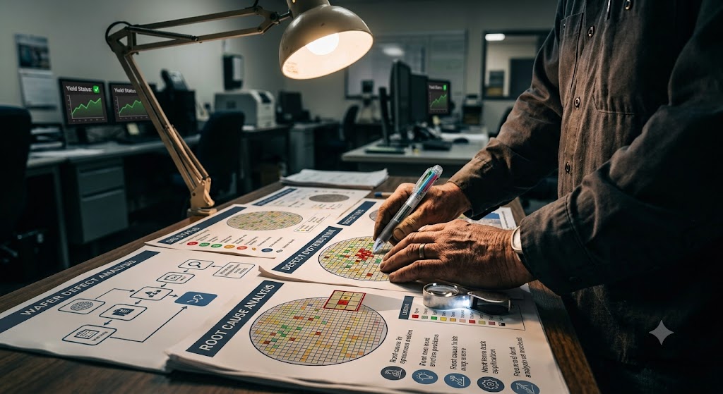
What he did first after arriving in Texas is also symbolic. Instead of ordering new equipment, it is known that he first reached out to several process engineers he had worked with during his time at Intel. It was a sequence of securing people before buildings. A semiconductor fab doesn’t run just because you put in the equipment. People who know how to handle that equipment must be in place before the building begins to function as a factory.
Nevertheless, Terafab has not yet found a top executive to oversee the entire project. They have been publicly recruiting for a Technical Program Manager since March, but industry observers say they have yet to find the right candidate. It takes time for transplanted organs to settle into a body. Sometimes they cause rejection reactions. Just bringing in a few Intel process experts doesn’t mean the habits accumulated over 40 years at TSMC and Intel will immediately take root at the new Texas site.
It’s not just new hires who are demanded to move at speed. One semiconductor equipment company representative received a request for a quote on a Friday, which was a holiday. The deadline was the following Monday. He must have spent the weekend poring over photomask or etcher specifications. That one person’s weekend is the reality of the speed this project demands.
Equipment itself is not abundant. The latest EUV lithography equipment needed for 2nm-class processes is supplied exclusively worldwide by ASML in the Netherlands. The annual production of this equipment, which costs $200 million per unit, is limited to around 30–50 units. There have been several years where they didn’t meet their target numbers. TSMC, Samsung, and Intel have already secured several years’ worth of supply. No matter how much Terafab rushes, there is equipment for which they must wait in line.
There is another debate surrounding process culture. Musk recently argued that traditional cleanroom design itself is wrong. He views the cost of air purification as a waste of resources and believes that hermetically sealing only the silicon wafer process area is sufficient.
“You can operate a 2nm fab while eating a cheeseburger and smoking a cigar.”
Advanced foundry cleanrooms are usually ISO Class 1–3. This means there must be fewer than 10 particles of 0.1 micrometers per cubic meter. A single streak of cigarette smoke would easily shatter this standard. Anyone who knows that a single speck of dust can ruin an entire wafer in the lithography process feels anxiety at this statement.
This isn’t the first gamble Musk has taken. At Battery Day in 2020, he promised to produce 100 gigawatt-hours of 4680 batteries annually by 2022 and lower costs by 56 percent. Five and a half years later, in 2025, actual production remained at around 20 gigawatt-hours per year. It is the industry’s common consensus that manufacturing battery cells is dozens of times simpler than advanced semiconductor manufacturing. Even in simpler manufacturing processes, the gap between goals and results was this large.
Water issues also remain. Terafab draws industrial water from the nearby Gibbons Creek Reservoir. Advanced processes consume massive amounts of ultrapure water. Texas is a region prone to drought, and water management agreements with the local community remain another variable for this project. The first thing residents asked at the public hearing was not about semiconductor technology, but about the reservoir’s water level.
If It Succeeds, If It Fails
The success scenario is clear. If Terafab hits its target yield, Tesla and SpaceX will be able to churn out as many chips as they want without worrying about outside foundries. A situation will open up where the mass production schedules for robotaxis and Optimus are determined solely by technology, not chip supply. The bottleneck for SpaceX’s space data center vision will also shift from launch vehicles to computing acquisition speed. For the industry as a whole, it means a third axis is created on the advanced foundry map, which has until now been concentrated on TSMC and Samsung.
The failure scenario is also distinct. A picture where they start with low yields and fail to ramp up for years, with only capital tied up. There is already a precedent. The gap between the 2020 Battery Day promises and the actual 2025 production is a microcosm of that. Semiconductors are a much more complex process than batteries. If the same pattern repeats, the $16.8 billion could remain just the beginning. In that case, it’s not just the investors who bear the loss. The plans to hire 3,000 people, the expectations for the local economy, and the Grimes County residents who signed water usage agreements will all share that result.
Industry skeptics also lean toward this failure scenario. A company with zero advanced foundry experience plans to complete the world’s largest fab within a few years. Many view this as “another Musk-style exaggeration.” Semiconductor industry insiders point out that it is normal for new fabs and chip designs to take months to years to reach the pilot stage. Some analyses suggest there is virtually no possibility of meaningful volume coming out within this year. Nevertheless, the reason this project continues to attract attention is that regardless of success or failure, the results will remain as a reference case for the entire industry.
Korea is Not a Spectator
There is a reason this story doesn’t just read like a story about a factory in another country. Tesla has already signed a contract with Samsung Electronics to receive AI semiconductors until 2033 and decided to produce next-generation AI6 chips at the Taylor, Texas plant. When Dojo was suspended, Tesla relied on Samsung and Intel. Until Terafab completes its own production system, a significant portion of Tesla’s chip demand is structured to be supported by Korean foundries.
At the same time, if Terafab actually reaches orbit, the situation will change. A flow where the initiative in semiconductor supply shifts from foundry-specialized companies to platform companies that use the chips directly will become distinct. Korean automotive and parts companies may also face a trigger to redraw supply strategies for their overseas production bases. The success or failure of Terafab will be decided at the site next to the Texas reservoir, but the scope of its impact is much wider.
Where Will They Get the People?
Gary Jiang alone cannot transfer an entire culture. That is why Terafab is currently scouring the globe for process personnel. Recruiters are contacting not only domestic semiconductor personnel but also engineers with experience working in overseas fabs. Moves to secure talent by visiting Seoul National University and KAIST to promote overseas working conditions have also been detected.
This isn’t just a Terafab phenomenon. Big Tech as a whole is engaged in a cross-border talent war over semiconductor and AI personnel. However, bringing in personnel individually and those people gathering to form a single organizational culture are different problems. TSMC’s 40 years were a time when the same people repeated the same failures and aligned their criteria for judgment. Just gathering people from different companies and different countries in one factory won’t compress that time.
At this point, the question is no longer “Will Terafab be completed?” The real question lies in a much broader place. Why does American advanced manufacturing, even with the world’s highest level of capital and talent, repeatedly trip and fall at this point?
Why Does American Manufacturing Repeatedly Get Stuck Here?
Tesla has already hit this wall once before. They tried to introduce a dry electrode process for batteries and suffered delays for years, and they had to redraw their plans whenever the supply chain shook. It is natural to ask if they can handle a much more sophisticated 2nm-class semiconductor process.
But this isn’t just a story about one company, Tesla. Large semiconductor companies that received government subsidies have also experienced a series of delays in factory construction and operation over the past few years. Advanced fabs slated for Texas, Arizona, and Ohio have all pushed back their completion dates several times. The capital was sufficient. They secured the sites. What was actually lacking was the organizational judgment to turn that capital into yield.
Intel’s situation shows something similar. Since taking office, Intel CEO Pat Gelsinger has emphasized simplification, rapid execution, and financial health. They succeeded in mass-producing the 18A process, but they struggled to find a large anchor customer to justify that capital expenditure. Industry interpretations suggest that Intel joining Terafab wasn’t about giving away technology for free, but because they needed a partner that would lead to actual profit. Even a company with the world’s highest-level process technology cannot justify capital expenditure if it doesn’t have a partner to prove that technology’s value in the market.
There is a deeper structure here. American manufacturing has been restructuring its organizations based on financial logic for the past several decades. Quarterly earnings became the standard for hiring and investment, and skilled field personnel were treated as cost items, not assets. When the economy worsened, these people were the first to be laid off. Semiconductor design remained in Silicon Valley, and the process personnel who actually move their hands to capture yield moved to Asia a long time ago.
The roots of this flow are quite old. In the 1990s and 2000s, major American corporations repeatedly chose to move production lines overseas and shrink R&D organizations to lower manufacturing costs. Places once considered the world’s best industrial research labs also downsized within this flow. These were decisions to increase short-term profit margins, but what disappeared in exchange was the organizational habit of enduring failure and digging into problems to the end. The US is now trying to fill the space where that habit disappeared. The problem is that while a few rounds of restructuring were enough to eliminate that habit, it takes much longer to revive it.
What TSMC and Samsung have built over 40 years is not a list of patents or equipment. It is a cycle where people who repeat failures and learn from them pass that judgment on to the next generation. Junior engineers watch and absorb the intuition as they see their seniors holding the line at 3 a.m. to find the cause for years. American manufacturing has broken this cycle several times. Terafab is close to an attempt to restore that broken cycle all at once with money and speed.
At the same time, this project is a microcosm of a national attempt by the US to regain semiconductor sovereignty. Musk has offered a prescription for the problem—that it’s not equipment or capital, but a collapsed field culture—in a different way. Recruiting Intel process experts one after another is, in the end, an attempt to urgently transplant that culture on a person-by-person basis.
This flow is not unique to the US. China has been pouring national-level investment for years, claiming it will complete advanced processes with only domestic equipment. Japan has established a national foundry called Rapidus and is running with the goal of 2nm mass production, and the EU is also trying to boost regional production through its own semiconductor act. The fact that each government has realized simultaneously is the same: Semiconductor production capacity is not a product you can buy with money, but a capability that must be cultivated over a generation. Yet, every country is trying to secure that capability within a few years, within an election cycle or a quarterly earnings cycle. Terafab is just the most extreme compression attempt among them.
Perhaps the question itself is wrong. Instead of asking whether Terafab will be completed in a few months or how quickly they will ramp up yields, we might need to ask a different question. The question is whether this kind of accumulation can be measured by the yardstick of ‘speed’ in the first place. Infrastructure like dams or rail networks wasn’t completed within a single generation. Semiconductor manufacturing capability might also be the kind of thing that doesn’t get completed on the timetable of quarterly earnings.
Whether the transplanted organ will take root or cause a rejection reaction—no one has the answer to this question yet. The point when the first phase of construction is finished and the first wafers emerge is discussed as being no earlier than 2027. The point when it is confirmed whether those wafers come out with usable yield is much later. What is certain is that the answer will come long after the concrete has been poured.
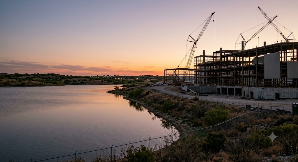
🖼️ Image Prompt (Replace the image above after generating): A quiet dusk photograph of a still reservoir beside a half-built industrial structure in rural Texas, warm fading light on the water, distant construction cranes silhouetted, documentary photography, contemplative mood, no people visible
When you want to build something quickly, have you ever asked what you can’t buy with money and speed? Whether it’s company performance, team skill, or trust between people—there are things that can only be built by spending time.
Terafab is just asking that question in the largest and most expensive way on Earth.
References
- Edaily Marketin, Musk's direct semiconductor production Terafab report
- Epoch Times, Tesla SpaceX Terafab launch report
- NewsN Union, Terafab Grimes County construction start report
- CIO, Intel-Musk cooperation Terafab promotion article
- TradingKey, Intel Terafab joining and foundry strategy analysis
- Future Korea, Terafab analysis article: Bluff or Miracle?
- SBS Premium, Terafab cleanroom and fool index explanation article
- Villain City, Musk cigar/cheeseburger cleanroom remark report
- Pressman, Terafab vs 4680 Battery Day comparative analysis
- ZDNet Korea, Gary Jiang Terafab Director appointment report
- AI Times, Intel veteran Gary Jiang recruitment detailed report
- AI Times, Dojo project suspension and DensityAI startup report
- iRobot News, Dojo 3 project restart report
- Newsis, ASML High-NA EUV supply shortage report
- Kyunghyang Shinmun, ASML EUV lithography monopoly structure explanation